
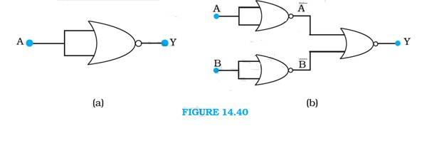
14.15 Write the truth table for the circuits given in Fig. 14.40 consisting of NOR gates only. Identify the logic operations (OR, AND, NOT) performed by the two circuits.
14.15 Write the truth table for the circuits given in Fig. 14.40 consisting of NOR gates only. Identify the logic operations (OR, AND, NOT) performed by the two circuits.

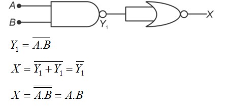
14.15 A acts as two inputs of the NOR gate and Y is the output. As shown in the following figure. Hence the output of the circuit is =

The truth table for the same is given as:
A | Y = ( ) |
0 | 1 |
1 | 0 |
This is the truth table of a NOT gate. Hence, this circuit functions as a NOT gate.
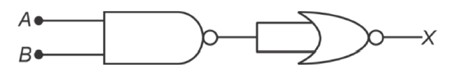
A and B are the inputs and Y is the ou
 Upvote
Similar Questions for you
A n-p-n transistor can be used as amplifier.

Corresponding binary numbers of given waveforms.
Taking an Exam? Selecting a College?
Get authentic answers from experts, students and alumni that you won't find anywhere else.
On Shiksha, get access to
Learn more about...

Physics Ncert Solutions Class 12th 2026
View Exam DetailsMost viewed information
SummaryDidn't find the answer you were looking for?
Search from Shiksha's 1 lakh+ Topics
Ask Current Students, Alumni & our Experts
Have a question related to your career & education?
See what others like you are asking & answering